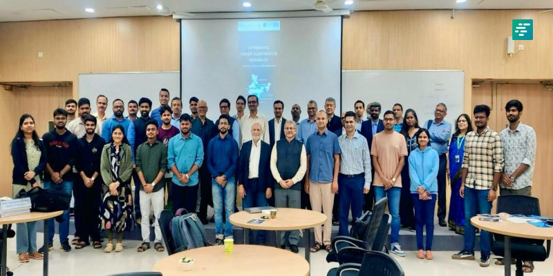
Indian Institute of Technology (IIT) Bhubaneswar hosted a one-day national workshop on “Setting Up a Pilot Line for Integrated Power Electronics” on 14th November 2025, bringing together leading representatives from industry, academia and government to advance India’s semiconductor ambitions under the India Semiconductor Mission (ISM). The workshop aimed to gather critical inputs for shaping the proposal for the Integrated Power Electronics Hub to be established at IIT Bhubaneswar.
In his address, Prof. Shreepad Karmalkar, Director, IIT Bhubaneswar, emphasised the national momentum and the need for strong collaboration under the India Semiconductor Mission. He said, “A nationwide effort is underway to build a robust Industry–Academia–Government partnership for a globally competitive semiconductor ecosystem. IIT Bhubaneswar, with its 936-acre scenic campus at the foot of Barunei Hill, is contributing significantly through its ₹64-crore SiC Research and Innovation Centre, its role in the upcoming 220-acre Semiconductor and ESDM Park, a year-long PG Diploma in Semiconductor Technology, and the newly sanctioned ₹4.95-crore NaMo Semiconductor Laboratory. Our M.Tech, MS and PhD programmes in semiconductor technology and chip design further strengthen India’s talent pipeline.”
Prof. Rao Tummala, Advisor to ISM, presented the purpose of the workshop, clarifying the two primary goals: establishing IIT Bhubaneswar as an Integrated Power Electronics Hub with a pilot line for industry prototypes, and setting up an industry consortium to extend existing package manufacturing lines across six states.
Mr. Ashok Chandak, President of Energy Storage Association in India (IESA) & Semiconductor Equipment and Materials International (SEMI) India showed the statistics of semiconductor growth in India. Also touched upon how the proposed hub is going to be set up and managed.
Sessions through the day included detailed presentations on the role of IIT Bhubaneswar in the national hub network, the organisation and management of the multi-institutional structure, and the responsibilities of each technology centre. Industry leaders then delivered short presentations showcasing their tools, technologies and materials essential for setting up the Integrated Power Electronics Hub at IIT Bhubaneswar. These covered a wide range of domains including design automation tools, board assembly reliability, thermal technologies, materials and components, substrates, power module design, and electrical testing.
In the afternoon, faculty leaders from Indian Design, Semiconductors, Packaging and Systems Program (IDSPS) presented thematic R&D areas aligned with the mission, followed by a session devoted to discussing the extension of existing manufacturing lines in India through industry partnerships. Prof. Satyam Parlapalli of IIT Bhubaneswar presented the initial proposal for the Integrated Power Electronics Pilot Facility at IIT Bhubaneswar, explaining the technological requirements and integration pathways across the participating national centres. A session on the support from the Government of Odisha (listed as tentative in the programme) was presented by Shri Vishal Kumar Dev, Principal Secretary of Electronics & IT Dept, Odisha, as part of the collaborative outlook for the proposed hub.
The workshop concluded with one-on-one networking discussions and an action-planning session outlining the next steps for preparing the funding proposal. The participants later toured IIT Bhubaneswar’s research facilities, gaining insight into the Institute’s infrastructure, including initiatives in wide-bandgap materials, power device characterization, and advanced semiconductor research capabilities.
